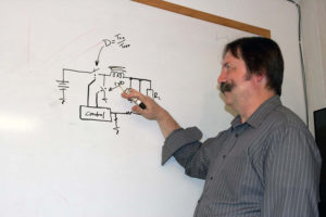
 RF and High Speed PCB and EMI Design Fundamentals
Course 042
Summary:
This two-day course enables practicing engineers and CAD technicians to develop design rules for RF and high-speed designs, choose an optimal design tool, and organize the design process to most efficiently execute the design that will insure circuit performance, and minimize costs and production time.
Learning Objectives:
Upon completing the course, the participant will be able to:
- Discuss fundamental RF and digital PCB design issues.
- Compare and contrast transmission lines types, characteristics, and situations in which they can be used.
- Describe, evaluate, and compare termination types, PCB materials and fabrication processes, and packaging types.
- Identify and compensate for sources of interference – EMI and EMC.
- Measure and fine-tune circuit performance.
Identify and select tools for developing transmission line design rules.
Target Audience:
Anyone working with RF circuits or high-speed digital logic, including RF engineers, digital logic engineers, technicians, and PCB layout professionals will benefit from this course. A practical engineering background and basic mathematics are required to follow the course.
Subject Areas Covered:
High-Speed PCB Layout and Design
EM Shielding/EMC Engineering
Signal Integrity of High-Speed Digital Design
Key Concepts:
Transmission Lines • Microstrip • Transmission Lines • Reflection Coefficient • PCB • Interference
• Crosstalk • Ground/Grounding